
Samsung Electronics, a leading provider of advanced semiconductor technology, has announced a reinforced business strategy for its Foundry Business with the launch of cutting-edge technologies at its annual Samsung Foundry Forum event.
The demand for advanced semiconductors has significantly increased due to the market growth in high-performance computing (HPC), artificial intelligence (AI), 5/6G connectivity, and automotive applications. As a result, innovation in semiconductor process technology is crucial for the commercial success of foundry customers.
Samsung emphasized during the event that it would begin mass producing products using its most cutting-edge process technology, 1.4-nanometer (nm), in 2027. Additionally, Samsung described the efforts its Foundry Business is taking to satisfy the needs of its clients, including foundry process technology innovation; process technology optimization for each particular application; stable production capabilities; and customized client services.

Samsung’s Advanced Node Roadmap Down to 1.4nm in 2027
Samsung will be further developing gate-all-around (GAA) based technology and has plans to introduce the 2nm process in 2025 and the 1.4nm process in 2027 as a result of the company’s achievement in delivering the most recent 3nm process technology to mass production.
Moreover, Samsung is advancing 2.5D/3D heterogeneous integration packaging technology while simultaneously setting the pace for process technology innovation to offer a complete system solution for foundry services. Its 3D packaging X-Cube with micro-bump connections will be accessible in mass production in 2024 thanks to ongoing research, and bump-less X-Cube will be available in 2026.
“Shell-First” Strategy in Response to Customer Demands
By 2027, compared to this year, Samsung wants to more than triple its production capacity for advanced nodes. Samsung presently has foundry production lines in five locations: Giheung, Hwaseong, and Pyeongtaek in Korea; Austin and Taylor in the United States; and the new fab being built in Taylor, Texas.
Samsung explained at the event how it builds cleanrooms first, regardless of market conditions, as part of its “Shell-First” capacity investment strategy. Cleanrooms are easily accessible, allowing for the flexible installation and configuration of fabrication equipment as needed to meet future demand.
Samsung will be able to better satisfy customer demands due to the new investment plan. Additionally, plans for an additional “Shell-First” manufacturing line in Taylor, which would follow the first line announced last year, as well as a prospective expansion of Samsung’s global semiconductor production network were also disclosed.
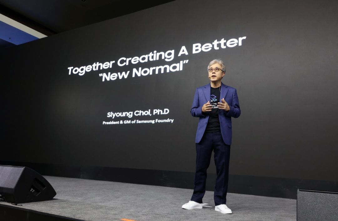
According to Dr. Si-young Choi, president and head of Foundry Business at Samsung Electronics, Samsung’s initiatives to win customers’ trust and help their success include the technical development objective down to 1.4nm, foundry platforms tailored for each application, dependable supply through persistent investment, and others. Their foundry service has always been focused on helping each customer and their partners realize their innovations.